Pre-FAB Academy
Week 3
Electronics and programming
Franc suggested to run our catch up plan and be back on track by friday.
Day 1 -Electronics Production
We downloaded board designs from fab academy archives. Roland Modela is used for milling the circuit board.
Preparing the Roland Modela
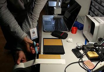
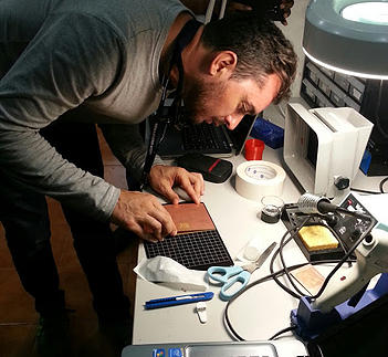
Change the bed to metal bed. Milling board is very sensitive to height, so place a sacrificial layer underneath. Metal board is used instead of acrylic sheet as the acrylic sheet has irregular shape. Copper plate is used as sacrificial layer upside down.
Fab foundation uses double sided scotch tape to fix the plate, but franc suggests to use white double sided tape.
Note: The copper gets rusted with touch. So, after milling take it for a wash to remove the rusting. Try not to use rusted plate for milling sensitive boards.
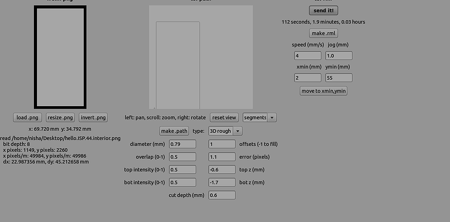
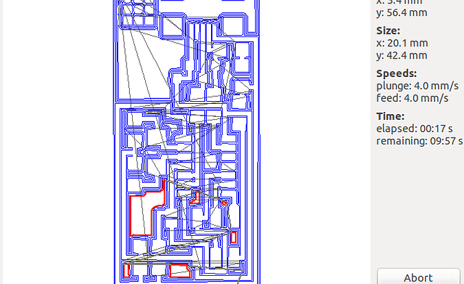
Put 1/64th bit on to the machine. Be careful to not drop the bit since it is very delicate. Load the .png file of the traces. Rotate the image and find a suitable area in the plate to mill the board and align the image accordingly by moving x axis and y axis accordingly. Just as in molding, set orgin, make path, make rml and send the image for milling. Make sure that the tool path generated is as per required.
After every change make path. After milling the traces, check for any path not being cut. This can happen when the bed is not flat. To avoid this the cut depth can be increased to 0.15 or 0.2mm. But this approach must be taken only if the milling is not done properly. Other wise this could stress the blade and result in damage of bit. After making rml, send the image for milling. Vacum the debris and verify the circuit board for any missing traces.
We encountered a problem of broken trace. This was due to the traces being very thin. If the traces gets removed off when rubbed then the circuit is not fit. For thicker lines, we downloaded another version of fabisp design (Neil version of fabisp).
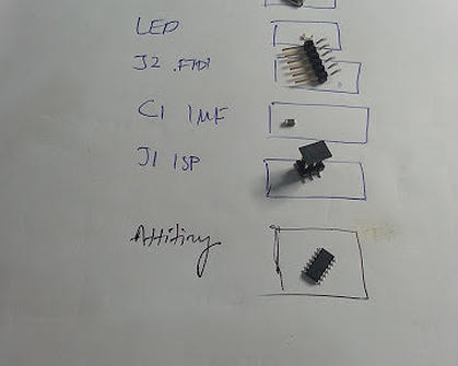
Components Required for the circuit board:
Take the circuit image. Take only one component at a time and place them properly marked in a paper to avoid jumbling up the components. Keep the box open until you keep back the strip after taking the component, this is an effective method to avoid mixing up components.
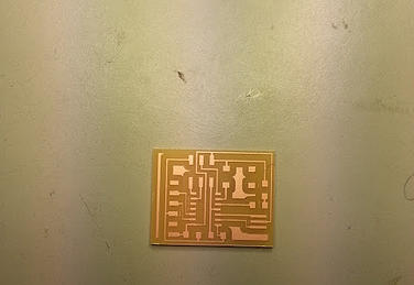
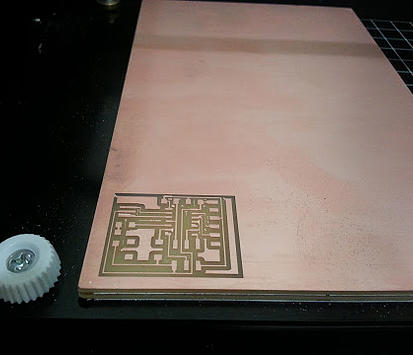
After milling the traces, The 1/64 bit is changed to 1/32 bit to mill the outline image. The outline image is loaded and the board is milled finally. The traces looks good and are thick enough. Now, we need to pry the board out which is stuck to the sacrificial layer by the double sided tape.
For removing use thin edged tools like screw driver and move the board slightly on all four corners. Once the board starts to move off, pry from the side which won't result in any harm for the circuit board. The board comes off with the double sided tape on, which we could use to keep the board firmly affixed to the desk while soldering.
Soldering:
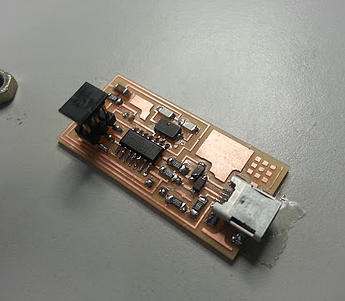
The components are soldered into the traces. The board is stuck onto the desk before soldering.
Things to note down while soldering :
-
Always solder from the middle of the board to the boundary.
-
Solder complex components at first
-
Heat up the soldering gun till the indicator light does not flicker and also keep the tip of the soldering gun clean.
-
The fume suction should always be on. The fumes that comes out during soldering might contain lead particles which is harmful to health.
-
At first, solder any one pin of the component to fix it to the trace.
-
Use tweezers to place the componenets in place and take extra care to align them properly
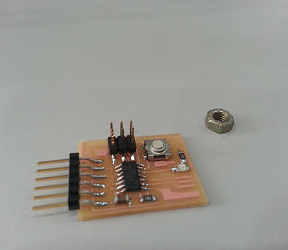
The final product.
Programming in fabisp
DAY 2 - Designing circuit
Today, we were supposed to design an electric circuit
and then produce it. I installed kokopelli in my ubuntu. Franc insists
us to use kokopelli instead of softwares such as kicad, eagle. Kokopelli
is more flexible and all the circuit drawing is based on equation.
Assignment for the day : To design an electric circuit in kokopelli, solder and produce it.
To open from terminal
-
go to: /home/nisha/koko_retro/bin
-
Right click and Open in terminal
Adding components into the circuit:
-
Add components into the circuit in right areas.
-
Add traces
-
Increase board size if required and reposition the elements if required.
From Line 3594 onwards the codes are defining the board, before that
each elements, circuit component and alphabets were defined.
So changing the board parameters should be done under the #define board paramenter
The code is
#
# define board
#
w = .016
width = 1
height = .93
mask = .004
x = 1
y = 1
z = -.005
d = .06
pcb = PCB(x,y,width,height,mask)
Note: Traces should be having a width of atleast 0.012mm.
After the board components and width is slightly varied these are the
Changes made in kokopelli to insert an LED, pullup resistor and Button.
LED1=LED_1206('led')
pcb=LED1.add(pcb,XTAL1.x,IC1.pad[5].y,z,180)
R2=R_1206('R2\n1k')
pcb=R2.add(pcb,LED1.pad[2].x,LED1.y-0.16,z,-90)
B1=button_6mm('B1')
pcb=B1.add(pcb,LED1.x+0.17,J1.y+0.05,z)
pcb = wire(pcb,w, #adding traces
IC1.pad[5],
LED1.pad[1])
pcb = wire(pcb,w,
LED1.pad[2],
R2.pad[1])
pcb = wire(pcb,w,
J1.pad[6],
R2.pad[2]
)
pcb = wire(pcb,w,
IC1.pad[6],
B1.pad[4]
)
pcb = wire(pcb,w,
J1.pad[6],
B1.pad[3]
)
Electronics components were taken and solder as we did for fabisp.
Day 3 - Embedded programming
For timing sensitive projects, with assembly we can do same thing as in arduino with less clock cycle. Arduino waste so much energy, clock cycle and not much efficient so deploy using c or assembly languages. Solution is way better and cheap with C and Assembly.
Arduino takes 4K of memory. But C and Assembly takes less.
Created circuit board with LED, button and RC filter with ATtiny44.
We then downloaded arduino IDE and opened arduino IDE from terminal. Attiny44 add-on was done in the arduino IDE and bootloader was burnt.
Programming
programming usually has two parts
1) SETUP or INIT – this is where we set all the variables in the program
2) LOOP – this is where the orginal process runs
Every pin in MC can deliever only 40mA tops.
Button switches between 0V and 5V.
Output can be digital. Input can be digital or analog values.
There are analog pins to read analog values. For doing this analog to digital converters are
For less precision use 8bit ADC (0-255)
For higher precision use 10bit ADC (0-1023)
Programming with the arduino
We blinked the LED with one second delay and then used the button to on/off the LED.
Then next we programmed the Attiny so that the LED turns ON when the button is pressed.
We programmed such that when the button is pressed, the Serial monitor shows “Press”
Programmed such that when an alphabet “c” sent through serial monitor the LED turns on.
Catch Up Plan:
My todays catch up plan was
-
Mill, Solder and make the circuit board with LED, Resistor and Button.
-
Make Mold design again in Antimony
-
Make the Re-Designed version of Hook in Antimony
-
Install Antimony in my laptop
The first three was done. But as usual I'm still facing problems in Installing antimony in my laptop which is due to having less RAM space it seems.
Day 4:
Controlling Boards directly with Computer or Mobile Devices.
Today, we were to control boards wirelessly from computers or mobile devices. Franc instructed to download MIT I2 App in mobiles.
We could not get in track as expected today, so I decided to follow the Catch up Plan until the lecture classes begins.
Today's Catch Up plan:
-
Mill Mould with the design made in Antimony yesterday.
-
Documentation and Site Updation.
Morning I came to fablab and started off with Documentation. Re-milled the mould since the previous mould did not have a clearance space of 5mm on top and the edges were thin.
So, we redesigned the mould again in antimony and milled the mould.
I was planning to do 3D printing of the hook I redesigned, but since we require a lot of hooks at the lab for hanging nameplates. It is better to create a mold of hook. Franc assigned micheal to create the mold of hook.
Video Conferencing
To communicate with remote guru you need to set up video conferencing. The line should have atleast 1Mbps uplink. A dedicated line is recommended for video conferencing.
There are two addresses to connect to mit mainframe
1) mcu.cba.mit.edu – has 80 ports, this is only for fab labs to connect
2) mcuc.cba.mit.edu – has 80 ports, this is for individual people to connect when you can't come to lab.
Shopbot basics were lectured
opendesk.cc – A useful site to get designs of furniture.
Tabs and Nesting
Cut2D
After making a design, the next design should be places along side. Do nesting, instead of wasting the acrylic or wood while cutting. Rotate, move designs manually to give a proper nesting and saving material.
Remember to close the polylines (line made of multiple lines by joining the individual lines).
If there are drills in design, do them first. Execute the drills first.
Tool paths – Mainly three types.
Drill
Don't screw everywhere in the wood. Only screw at the edges. Otherwise, chances are there that the bit breaks while passing through the screw area.
To create cavities and pockets. This must be the second instruction done.
Cut
Cuts needs to be manually suggested to the shopbot. The interior cuts should be done at first and then do the exterior cuts.
Problems faced by Shopbot:
-
Placing of milling bit
To mill or cut exterior areas, the bit should be placed at exterior.
To mill or cut interior areas, the bit should be placed in the interior.
Milling bit can be placed in the middle too.
-
Take care that while cutting rounded edges doesn't happen.
Cut3D
It is mostly used for 3D cutting of moulds.
There are two paths, like in wax moulding. Rough and finish path.
Rough path for rough cut. Finish path can be done by assigning in grids of various angles. There is no need of much detailing.
Downloaded Ekiga – to do voip calls and video conferencing
Learnt about Desktop Sharing – so that desktop can be shared with remote guru for debugging purposes.
Day 5
Basics of shop bot was covered on the day. The Shopbot is a large milling machine for cutting, phrasing and shaping wood and plastic in various 3-dimensional sizes.
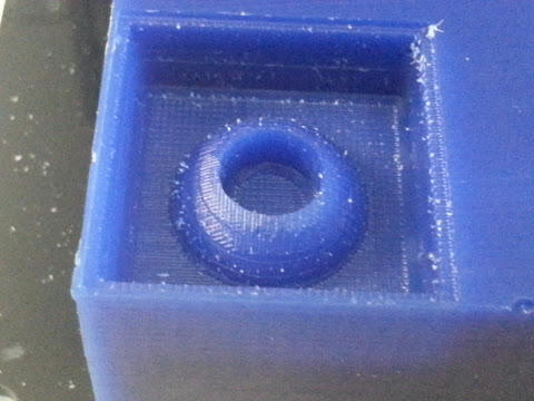
Also, I milled another mould with a figure of difference between sphere and a cylinder
Catch up plan was to complete off with this weeks documentation works.
DOCUMENTATION
My journey through the Pre- Fab Academy workshop...
